5,000 Tiny Bridges: The Invisible Engineering Marvel Inside Your Smartphone
The hidden lattice that powers – and melts – your gadgets.
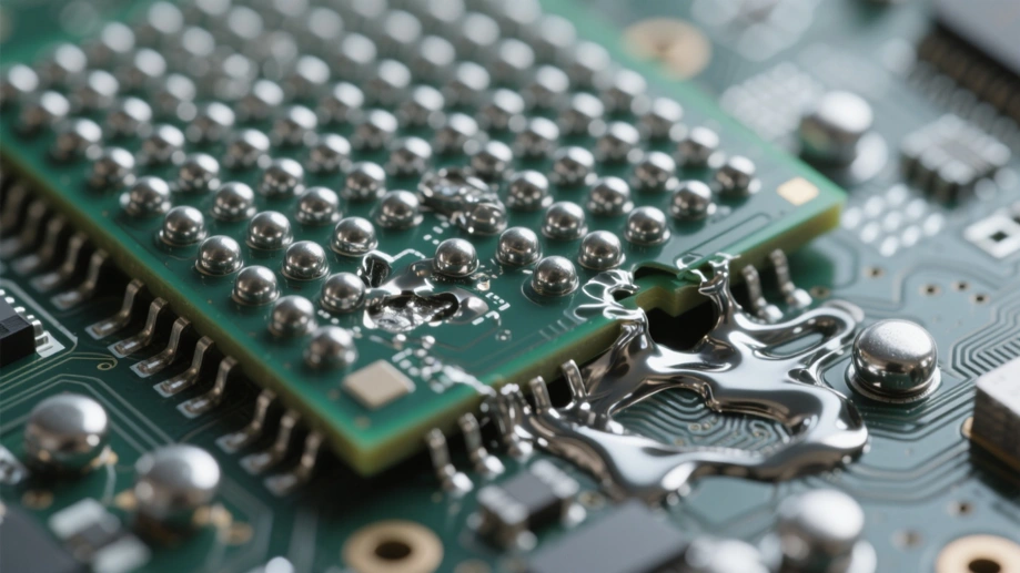
Ever wondered how the brain of your smartphone, that sophisticated chip smaller than your thumbnail, talks to the rest of its electronic body? It's not magic, but an often-overlooked feat of engineering called Ball Grid Array packaging, and its tiny solder balls hold the key. These microscopic metallic spheres, numbering in the thousands, form a critical bridge between the silicon die and the printed circuit board (PCB), carrying power and signals vital for your device to function. Without this dense forest of miniature bridges, modern electronics simply couldn't exist.
Think of it like constructing an ultra-miniature city. The chip is the bustling downtown core, packed with transistors handling billions of calculations every second. The PCB is the sprawling suburbs and infrastructure – the memory lanes, power supply stations, and signal highways. The Ball Grid Array (BGA) is the intricate network of bridges and tunnels connecting downtown to the suburbs. Each tiny solder ball serves as a single point of connection, an electrical conduit and a physical anchor. The sheer density of these connections, cramming thousands onto a surface area smaller than a postage stamp, enables the incredibly complex communication required by today's processors.
But here’s the catch: these vital bridges are incredibly vulnerable to heat. Your phone heating up during intensive gaming or video streaming isn't just uncomfortable for you; it's a serious stress test for those solder balls. As the chip and PCB heat up, they expand. Different materials expand at different rates – a concept called the Coefficient of Thermal Expansion (CTE). The silicon chip expands very little, while the fiberglass PCB expands more. The tiny solder balls sandwiched between them are caught in this thermal tug-of-war.
Imagine thousands of miniature bridges constantly stretching and compressing with every heat cycle – turning the device on, pushing it hard, letting it cool down. This relentless thermal cycling is the primary cause of a notorious failure known as ‘solder joint fatigue’. Over time, micro-cracks can develop in the solder connections, especially around the outermost balls which experience the greatest mechanical stress. Like metal fatigue weakening a bridge cable, these cracks eventually grow, leading to intermittent glitches or complete failure – the infamous 'black screen of death' or a device that mysteriously stops charging. This hidden vulnerability is a major headache for hardware engineers.
So, how do engineers combat this invisible threat? The answer lies in constant material science innovation and meticulous thermal management inside your devices. On the material front, researchers and manufacturers continuously develop advanced solder alloys. Standard solder melts relatively easily, but newer formulations might incorporate tiny amounts of elements like silver, copper, or even indium to improve mechanical strength and fatigue resistance. Some solutions involve adding microscopic structures *within* the solder balls or using sophisticated underfill materials injected around the BGA to provide extra support and distribute stress.
Beyond the solder itself, keeping the whole device cooler is paramount. That's why you find heat sinks – often copper plates or vapor chambers – strategically placed on top of the main processor chips. These act like radiators, pulling heat away from the delicate solder joints as fast as possible. Thermal interface materials (grey pastes or pads you might see during teardowns) ensure efficient heat transfer from the chip surface to the heat sink. Cooling fans in larger devices like laptops also play a crucial role. Every degree shaved off the peak operating temperature significantly extends the life of those thousands of tiny solder bridges.
The implications ripple far beyond just fixing a broken phone. Understanding BGA technology and its limitations shapes global manufacturing and industry practices. The precision required to place thousands of balls perfectly demands multi-million-dollar pick-and-place machines equipped with sophisticated vision systems. This drives constant innovation in automation. The demand for higher performance chips pushes packaging towards even smaller ball pitches (the distance between centers of neighboring balls), demanding cleaner production environments to avoid microscopic contaminants causing shorts. This relentless miniaturization forms the backbone of Moore's Law marching forward.
Furthermore, awareness of thermal failure modes influences product design across the tech landscape. Consider automotive electronics, where components under the dash can face scorching temperatures. Or servers in data centers running 24/7 – their reliability hinges on robust thermal management strategies born from lessons learned in consumer electronics BGA failures. A tiny failure in a single solder ball can cascade into significant downtime and cost. This invisible engineering challenge silently shapes the reliability standards for countless industries.
Next time you feel your device warm up, remember the microscopic army of solder balls working furiously inside. Their strength and stability, forged through advanced materials and clever cooling, are what make your digital world tick. This unassuming lattice of connections, hidden beneath the surface, exemplifies how profound engineering challenges in miniature drive the evolution of technology we use every single day.